Piedinature - Pinouts
PCI
Torna alla Home Page di JackTorna alla pagina delle informazioni tecniche
Torna alla pagina dei Pinouts
Reference and Sources:
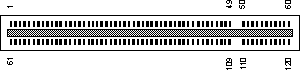
Main source: Copyrighted document from MARK SOKOS (sokos@desupernet.net - http://users.desupernet.net/sokos) PCI=Peripheral Component Interconnect This file is not intended to be a thorough coverage of the PCI standard. It is for informational purposes only, and is intended to give designers and hobbyists an overview of the bus so that they might be able to design their own PCI cards. Thus, I/O operations are explained in the most detail, while memory operations, which will usually not be dealt with by an I/O card, are only briefly explained. Hobbyists are also warned that, due to the higher clock speeds involved, PCI cards are more difficult to design than ISA cards or cards for other slower busses. Many companies are now making PCI prototyping cards, and, for those fortunate enough to have access to FPGA programmers, companies like Xilinx are offering PCI compliant designs which you can use as a starting point for your own projects. PCI Universal Card 32/64 bit ---------------------------------------------------------------- | PCI Component Side (side B) | | | | | | optional | | ____ mandatory 32-bit pins 64-bit pins _____| |___| |||||||--|||||||||||||||||--|||||||--|||||||||||||| ^ ^ ^ ^ ^ ^ ^ ^ b01 b11 b14 b49 b52 b62 b63 b94 PCI 5V Card 32/64 bit | optional | | ____ mandatory 32-bit pins 64-bit pins _____| |___| ||||||||||||||||||||||||||--|||||||--|||||||||||||| PCI 3.3V Card 32/64 bit | optional | | ____ mandatory 32-bit pins 64-bit pins _____| |___| |||||||--||||||||||||||||||||||||||--||||||||||||||
98+22 PIN EDGE CONNECTOR at the computer.
Notes: Pin 63-94 exists only on 64 bit PCI implementations. +V I/O is 3.3V on 3.3V boards, 5V on 5V boards, and define signal rails on the Universal board. Signal Descriptions:AD(x)Address/Data Lines. CLKClock. 33 MHz maximum. C/BE(x)Command, Byte Enable. FRAMEUsed to indicate whether the cycle is an address phase or a data phase. DEVSELDevice Select. IDSELInitialization Device Select INT(x)Interrupt IRDYInitiator Ready LOCKUsed to manage resource locks on the PCI bus. REQRequest. Requests a PCI transfer. GNTGrant. indicates that permission to use PCI is granted. PARParity. Used for AD0-31 and C/BE0-3. PERRParity Error. RSTReset. SBOSnoop Backoff. SDONESnoop Done. SERRSystem Error. Indicates an address parity error for special cycles or a system error. STOPAsserted by Target. Requests the master to stop the current transfer cycle. TCKTest Clock TDITest Data Input TDOTest Data Output TMSTest Mode Select TRDYTarget Ready TRSTTest Logic Reset The PCI bus treats all transfers as a burst operation. Each cycle begins with an address phase followed by one or more data phases. Data phases may repeat indefinitely, but are limited by a timer that defines the maximum amount of time that the PCI device may control the bus. This timer is set by the CPU as part of the configuration space. Each device has its own timer (see the Latency Timer in the configuration space). The same lines are used for address and data. The command lines are also used for byte enable lines. This is done to reduce the overall number of pins on the PCI connector. The Command lines (C/BE3 to C/BE0) indicate the type of bus transfer during the address phase.
The three basic types of transfers are I/O, Memory, and Configuration. PCI timing diagrams:___ ___ ___ ___ ___ ___ CLK ___| |___| |___| |___| |___| |___| |___ _______ _________ FRAME |_________________________________| ______ _______ ______ ______ ______ AD -------<______><_______><______><______><______>--- Address Data1 Data2 Data3 Data4 ______ _______________________________ C/BE -------<______><_______________________________>--- Command Byte Enable Signals ____________ ___ IRDY |_________________________________| _____________ ___ TRDY |________________________________| ______________ ___ DEVSEL |_______________________________| PCI transfer cycle, 4 data phases, no wait states. Data is transferred on the rising edge of CLK. [1] [2] [3] ___ ___ ___ ___ ___ ___ ___ ___ CLK ___| |___| |___| |___| |___| |___| |___| |___| |__ _______ _________ FRAME |________________________________________________| A B C ______ ______________ ______ _____________ AD -------<______>---------<______________><______><_____________>--- Address Data1 Data2 Data3 ______ ______________________________________________ C/BE -------<______><______________________________________________>--- Command Byte Enable Signals Wait ____________ _____ ___ IRDY |__________________________________| |_______| Wait Wait ______________________ ______ ___ TRDY |_______| |_______________________| ______________ ___ DEVSEL |______________________________________________| PCI transfer cycle, with wait states. Data is transferred on the rising edge of CLK at points labelled A, B, and C. Bus Cycles:Interrupt Acknowledge (0000)The interrupt controller automatically recognizes and reacts to the INTA (interrupt acknowledge) command. In the data phase, it transfers the interrupt vector to the AD lines. Special Cycle (0001)
I/O Read (0010) and I/O Write (0011)Input/Output device read or write operation. The AD lines contain a byte address (AD0 and AD1 must be decoded). PCI I/O ports may be 8 or 16 bits. PCI allows 32 bits of address space. On IBM compatible machines, the Intel CPU is limited to 16 bits of I/O space, which is further limited by some ISA cards that may also be installed in the machine (many ISA cards only decode the lower 10 bits of address space, and thus mirror themselves throughout the 16 bit I/O space). This limit assumes that the machine supports ISA or EISA slots in addition to PCI slots. The PCI configuration space may also be accessed through I/O ports 0x0CF8 (Address) and 0x0CFC (Data). The address port must be written first. Memory Read (0110) and Memory Write (0111)A read or write to the system memory space. The AD lines contain a doubleword address. AD0 and AD1 do not need to be decoded. The Byte Enable lines (C/BE) indicate which bytes are valid. Configuration Read (1010) and Configuration Write (1011)A read or write to the PCI device configuration space, which is 256 bytes in length. It is accessed in doubleword units. AD0 and AD1 contain 0, AD2-7 contain the doubleword address, AD8-10 are used for selecting the addressed unit a the malfunction unit, and the remaining AD lines are not used. Address Bit 32 16 15 0 00 Unit ID | Manufacturer ID 04 Status | Command 08 Class Code | Revision 0C BIST | Header | Latency | CLS 10-24 Base Address Register 28 Reserved 2C Reserved 30 Expansion ROM Base Address 34 Reserved 38 Reserved 3C MaxLat|MnGNT | INT-pin | INT-line 40-FF available for PCI unit Multiple Memory Read (1100)This is an extension of the memory read bus cycle. It is used to read large blocks of memory without caching, which is beneficial for long sequential memory accesses. Dual Address Cycle (1101)Two address cycles are necessary when a 64 bit address is used, but only a 32 bit physical address exists. The least significant portion of the address is placed on the AD lines first, followed by the most significant 32 bits. The second address cycle also contains the command for the type of transfer (I/O, Memory, etc). The PCI bus supports a 64 bit I/O address space, although this is not available on Intel based PCs due to limitations of the CPU. Memory-Read Line (1110)This cycle is used to read in more than two 32 bit data blocks, typically up to the end of a cache line. It is more efficient than normal memory read bursts for a long series of sequential memory accesses. Memory Write and Invalidate (1111)This indicates that a minimum of one cache line is to be transferred. This allows main memory to be updated, saving a cache write-back cycle. For more information seePCI Notes |
 (At the computer)
Torna alla Home Page di Jack
Torna alla pagina delle informazioni tecniche
Torna alla pagina dei Pinouts
(C) 2003-2025 Jack Mauro - electro.it