Piedinature - Pinouts
Communication and Networking Riser (CNR)
Torna alla Home Page di JackTorna alla pagina delle informazioni tecniche
Torna alla pagina dei Pinouts
Reference and Sources: The CNR connector is the interface between the motherboard and the CNR board. The connector provides all of the necessary signals to support several different configurations of audio, modem, and/or LAN subsystems in the system.
|
| Pin | Signal | Type | Description |
|---|---|---|---|
| A1 | RESERVED | - | RESERVED |
| B1 | RESERVED | - | RESERVED |
| A2 | RESERVED | - | RESERVED |
| B2 | RESERVED | - | RESERVED |
| A3 | GND | - | Power supply and signal ground return path. |
| B3 | RESERVED | - | RESERVED |
| A4 | RESERVED | - | RESERVED |
| B4 | GND | - | Power supply and signal ground return path. |
| A5 | RESERVED | - | RESERVED |
| B5 | RESERVED | - | RESERVED |
| A6 | GND | - | Power supply and signal ground return path. |
| B6 | RESERVED | - | RESERVED |
| A7 | LAN_TXD2 | IN | Bit 2 (MSB) of the 3-bit data bus transferring data from the MAC to the LAN Interface compliant PLC. For detailed information on this signal, refer to the current version of the Core Logic Design Specification. The reset state of this signal must meet the requirements set forth in the current version of the Core Logic Design Specification. |
| B7 | GND | - | Power supply and signal ground return path. |
| A8 | LAN_TXD0 | IN | Bit 0 (LSB) of the 3-bit data bus transferring data from the MAC to the LAN Interface compliant PLC. For detailed information on this signal, refer to the current version of the Core Logic Design Specification. The reset state of this signal must meet the requirements set forth in the current version of the Core Logic Design Specification. |
| B8 | LAN_TXD1 | IN | Bit 1 of the 3-bit data bus transferring data from the MAC to the LAN Interface compliant PLC. For detailed information on this signal, refer to the current version of the Core Logic Design Specification. The reset state of this signal must meet the requirements set forth in the current version of the Core Logic Design Specification. |
| A9 | GND | - | Power supply and signal ground return path. |
| B9 | LAN_RSTSYNC | OUT | This is a dual function pin that provides either a reset pulse or a synchronization pulse from the MAC to the LAN Interface compliant PLC. For detailed information on this signal, refer to the current version of the Core Logic Design Specification. The reset state of this signal must meet the requirements set forth in the current version of the Core Logic Design Specification. |
| A10 | LAN_CLK | OUT | Data clock from a LAN Interface compliant PLC to the Media Access Controller (MAC). The nominal frequency of this signal determines the data transfer rate between the PLC and the MAC. For detailed information, refer to the current version Core Logic Design Specification. The reset state of this signal must meet the requirements set forth in the current version of the Core Logic Design Specification. |
| B10 | GND | - | Power supply and signal ground return path. |
| A11 | LAN_RXD1 | OUT | Bit 1 of the 3-bit data bus transferring data from the LAN Interface compliant PLC device to the MAC. For detailed information on this signal, refer to the current version of the Core Logic Design Specification. The reset state of this signal must meet the requirements set forth in the current version of the Core Logic Design Specification. |
| B11 | LAN_RXD2 | OUT | Bit 2 (MSB) of the 3-bit data bus transferring data from the LAN Interface compliant PLC to the MAC. For detailed information on this signal, refer to the current version of the Core Logic Design Specification. The reset state of this signal must meet the requirements set forth in the current version of the Core Logic Design Specification. |
| A12 | RESERVED | - | RESERVED |
| B12 | LAN_RXD0 | OUT | Bit 0 (LSB) of the 3-bit data bus transferring data from the LAN Interface compliant PLC device to the MAC. For detailed information on this signal, refer to the current version of the Core Logic Design Specification. The reset state of this signal must meet the requirements set forth in the current version of the Core Logic Design Specification. |
| A13 | USB+ | IN/OUT | Positive side of the differential USB 1.x or 2.0 data signal. For more information, refer to the Universal Serial Bus Specification. The state of this signal during reset must meet the Universal Serial Bus Specification. |
| B13 | GND | - | Power supply and signal ground return path. |
| A14 | GND | - | Power supply and signal ground return path. |
| B14 | RESERVED | - | RESERVED |
| A15 | USB- | IN/OUT | Negative side of the differential USB 1.x or 2.0 data signal. For more information, refer to the Universal Serial Bus Specification. The state of this signal during reset must meet the Universal Serial Bus Specification. |
| B15 | +5Vdual | Supply | Positive 5-volt main/standby power supply (can be used for USB power). +5Vdual supply provides full-rated power capacity during working or full-on state, and a limited power capacity during sleep or suspended states. When a +5Vdual supply is not available, this pin must be connected to a +5 volt standby power source. This signal must not be connected to a +5VD, as doing so eliminates the possibility of deep-sleep wake capabilities. |
| A16 | +12V | Supply | Positive 12-volt main power supply |
| B16 | USB_OC# | OUT | USB bus over-current signal. For more information, refer to the Universal Serial Bus Specification. The state of this signal during reset must meet the Universal Serial Bus Specification. |
| A17 | GND | - | Power supply and signal ground return path. |
| B17 | GND | - | Power supply and signal ground return path. |
| A18 | +3.3Vdual | Supply | Positive 3.3-volt main/standby power supply. +3.3Vdual supply provides full-rated power capacity during working or full-on state, and a limited power capacity during sleep or suspended states. When +3.3Vdual is not available, this pin must be connected to a +3.3-volt standby power source. This signal must not be connected to a +3.3VD, as doing so eliminates the possibility of deep-sleep wake capabilities. |
| B18 | -12V | Supply | Negative 12-volt main power supply |
| A19 | +5VD | Supply | Positive 5-volt main digital power supply |
| B19 | +3.3VD | Supply | Positive 3.3-volt main digital power supply |
| A20 | GND | - | Power supply and signal ground return path. |
| B20 | GND | - | Power supply and signal ground return path. |
| A21 | EE_DIN | IN | This signal carries serial data from the core logic MAC Microwire* interface to the Microwire EEPROM (which stores MAC/PLC/PHY specific information) on the CNR board. The EE_DIN signal on the CNR connector must be connected to the DIN pin on the Microwire EEPROM. |
| B21 | EE_DOUT | OUT | This signal carries serial data from the Microwire EEPROM (which stores MAC/PLC/PHY specific information) on the CNR board to the core logic MAC Microwire* interface. The EE_DOUT signal on the CNR connector must be connected to the DOUT pin on the Microwire EEPROM. |
| A22 | EE_CS | IN | The CNR board uses this signal to enable the serial EEPROM devices on the CNR board. When EE_CS is high (one) the Microwire EEPROM (for the LAN Interface) becomes active. When EE_CS is low (zero) the EEPROM is inactive. The resting state of this signal is low (zero). The state of this signal during reset must be low (zero). |
| B22 | EE_SHCLK | IN | This signal is the serial clock signal from the core logic MAC Microwire* interface to the Microwire EEPROM (which stores MAC/PLC/PHY specific information) on the CNR board. |
| A23 | SMB_A1 | IN | This signal is bit 1 of the 3-bit address of the SMBus EEPROM on the CNR board. Refer to Section 6.1.1.2 for detailed information on the connectivity of this signal. The state of this signal during reset must be the SMBus address for the CNR board. |
| B23 | GND | - | Power supply and signal ground return path. |
| A24 | SMB_A2 | IN | This signal is bit 2 (MSB) of the 3-bit address of the SMBus EEPROM on the CNR board. Refer to Section 6.1.1.2 for detailed information on the connectivity of this signal. The state of this signal during reset must be the SMBus address for the CNR board. |
| B24 | SMB_A0 | IN | This signal is bit 0 (LSB) of the 3-bit address of the SMBus EEPROM on the CNR board. Refer to Section 6.1.1.2 for detailed information on the connectivity of this signal. The state of this signal during reset must be the SMBus address of the CNR board. |
| A25 | SMB_SDA | IN/OUT | Bi-directional serial data line between the SMBus master to SMBus slave device(s) on the CNR board. For detailed information on this signal, refer to the current version of the System Management Bus Specification. The reset state of this signal must meet the current version of the System Management Bus Specification. |
| B25 | SMB_SCL | IN | Serial clock line from the SMBus master to SMBus slave device(s) on the CNR board. For detailed information on this signal, refer to the current version of the System Management Bus Specification. The reset state of this signal must meet the current version of the System Management Bus Specification. |
| A26 | AC97_RESET# | IN | Active low AC TM97 link reset signal. For detailed information, refer to the current version of the AC TM97 Component Specification. The reset state of this signal must meet the requirements of the current version of the AC TM97 Component Specification. |
| B26 | CDC_DN_ENAB# | IN/OUT | CDC_DN_ENAB# indicates whether the motherboard or the CNR is in control, or mastering, the AC TM97 interface attached to the CNR Connector. When at a logic low level, the CDC_DN_ENAB# signal indicates that the primary codec on the motherboard is active and controlling the AC TM97 Interface. In addition, the CNR will, when CDC_DN_ENAB# is low, demote its codecs to the next available address and to the next available SDATA_IN signal. See Section 3.3.1 for more details on the implementation of the CDC_DN_ENAB# signal. When at a logic high level, the CDC_DN_ENAB# signal indicates that a primary codec on the CNR is taking control of the AC TM97 Interface. In addition, the motherboard will, when CDC_DN_ENAB# is high, disable all of its codecs. See Section 3.3.1 for more details of how to implement the CDC_DN_ENAB# signal. |
| A27 | RESERVED | - | RESERVED |
| B27 | GND | - | Power supply and signal ground return path. |
| A28 | AC97_SDATA_IN1 | OUT | AC TM97 serial data from an AC TM97-compliant codec (primary or secondary) to an AC TM97-compliant Controller. For detailed information, refer to the current version of the AC TM97 Component Specification. The reset state of this signal must meet the requirements of the current version of the AC TM97 Component Specification. |
| B28 | AC97_SYNC | IN | Synchronization pulse from an AC TM97-compliant controller to all of the AC TM97- compliant codecs on the AC link. This signal is nominally a 1.3 µS wide pulse, which is used to synchronize the AC link. For detailed information, refer to the current version of the AC TM97 Component Specification. The reset state of this signal must meet the requirements of the current version of the AC TM97 Component Specification. |
| A29 | AC97_SDATA_IN0 | OUT | AC TM97 serial data from a primary AC TM97-compliant codec to an AC TM97-compliant Controller. For detailed information, refer to the current version of the AC TM97 Component Specification. The reset state of this signal must meet the requirements of the current version of the AC TM97 Component Specification. |
| B29 | AC97_SDATA_OUT | IN | AC TM97 serial data from an AC TM97-compliant controller to all of the AC TM97- compliant codecs on the link. For detailed information, refer to the current version of the AC TM97 Component Specification. The reset state of this signal must meet the requirements of the current version of the AC TM97 Component Specification. |
| A30 | GND | - | Power supply and signal ground return path. |
| B30 | AC97_BITCLK | IN/OUT | Serial data clock from primary codec to AC TM97 Controller and any non-primary codecs. The nominal frequency of this signal is 12.288 MHz. For detailed information, refer to the current version of the AC TM97 Component Specification. AC97_BITCLK is an output from a primary codec and an input to non-primary codecs. The reset state of this signal must meet the requirements of the current version of the AC TM97 Component Specification. |
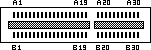
 Type B CNR connector
| Pin | Signal | Type | Description |
|---|---|---|---|
| A1 | MII_MDC | IN | Management data clock signal from Management Data Controller to the MII compliant PHY. For detailed information on this signal, refer to the current version of the Core Logic Design Specification and the IEEE 802.3u Specification. The reset state of this signal must meet the requirements set forth in the current version of the Core Logic Design Specification. |
| B1 | MII_MDIO | IN/OUT | Management data input/output signal between the Management Data Controller and the MII compliant PHY. This signal is used to carry bi-directional data for control and status registers. For detailed information on this signal, refer to the current version of the Core Logic Design Specification and the IEEE 802.3u Specification. The reset state of this signal must meet the requirements set forth in the current version of the Core Logic Design Specification. |
| A2 | MII_CRS | OUT | Carrier sense signal from the MII compliant PHY to the MAC. This signal indicates that there is traffic on the LAN wire. For detailed information on this signal, refer to the current version of the Core Logic Design Specification and the IEEE 802.3u Specification. The reset state of this signal must meet the requirements set forth in the current version of the Core Logic Design Specification. |
| B2 | MII_COL | OUT | Collision detect signal from the MII compliant PHY to the MAC. This signal indicates that a collision has occurred on the LAN wire. For detailed information on this signal, refer to the current version of the Core Logic Design Specification and the IEEE 802.3u Specification. The reset state of this signal must meet the requirements set forth in the current version of the Core Logic Design Specification. |
| A3 | GND | - | Power supply and signal ground return path. |
| B3 | MII_TXC | OUT | Data clock from the MAC to the MII compliant PHY. For detailed information, refer to the current version Core Logic Design Specification and the IEEE 802.3u Specification. The reset state of this signal must meet the requirements set forth in the current version of the Core Logic Design Specification. |
| A4 | MII_RXDV | OUT | Receive data valid signal from the MII compliant PHY to the MAC. This signal indicates that valid data is available on the MII_RXD[3:0] signals. For detailed information on this signal, refer to the current version of the Core Logic Design Specification and the IEEE 802.3u Specification. The reset state of this signal must meet the requirements set forth in the current version of the Core Logic Design Specification. |
| B4 | GND | - | Power supply and signal ground return path. |
| A5 | MII_RXC | OUT | Data clock from a MII Interface compliant PHY to the MAC. For detailed information, refer to the current version Core Logic Design Specification and the IEEE 802.3u Specification. The reset state of this signal must meet the requirements set forth in the current version of the Core Logic Design Specification. |
| B5 | MII_RXERR | OUT | Receive error signal from the MII compliant PHY to the MAC. This signal indicates that an error has occurred during frame reception. For detailed information on this signal, refer to the current version of the Core Logic Design Specification and the IEEE 802.3u Specification. The reset state of this signal must meet the requirements set forth in the current version of the Core Logic Design Specification. |
| A6 | GND | - | Power supply and signal ground return path. |
| B6 | MII_TXD3 | IN | Bit 3 (MSB) of the 4-bit data bus transferring data from the MAC to the MII compliant PHY. For detailed information on this signal, refer to the current version of the Core Logic Design Specification and the IEEE 802.3u Specification. The reset state of this signal must meet the requirements set forth in the current version of the Core Logic Design Specification. |
| A7 | MII_TXD2 | IN | Bit 2 of the 4-bit data bus transferring data from the MAC to the MII compliant PHY. For detailed information on this signal, refer to the current version of the Core Logic Design Specification and the IEEE 802.3u Specification. The reset state of this signal must meet the requirements set forth in the current version of the Core Logic Design Specification. |
| B7 | GND | - | Power supply and signal ground return path. |
| A8 | MII_TXD0 | IN | Bit 0 (LSB) of the 4-bit data bus transferring data from the MAC to the MII compliant PHY. For detailed information on this signal, refer to the current version of the Core Logic Design Specification and the IEEE 802.3u Specification. The reset state of this signal must meet the requirements set forth in the current version of the Core Logic Design Specification. |
| B8 | MII_TXD1 | IN | Bit 1 of the 4-bit data bus transferring data from the MAC to the MII compliant PHY. For detailed information on this signal, refer to the current version of the Core Logic Design Specification and the IEEE 802.3u Specification. The reset state of this signal must meet the requirements set forth in the current version of the Core Logic Design Specification. |
| A9 | GND | - | Power supply and signal ground return path. |
| B9 | MII_TXEN | IN | Transmit enable signal from the MAC to the MII compliant PHY. This signal indicates that the available on the MII_TXD[3:0] signals can be placed on the LAN wire. For detailed information on this signal, refer to the current version of the Core Logic Design Specification and the IEEE 802.3u Specification. The reset state of this signal must meet the requirements set forth in the current version of the Core Logic Design Specification. |
| A10 | RESERVED | - | RESERVED |
| B10 | GND | - | Power supply and signal ground return path. |
| A11 | MII_RXD1 | OUT | Bit 1 of the 4-bit data bus transferring data from the MII compliant PHY to the MAC. For detailed information on this signal, refer to the current version of the Core Logic Design Specification and the IEEE 802.3u Specification. The reset state of this signal must meet the requirements set forth in the current version of the Core Logic Design Specification. |
| B11 | MII_RXD2 | OUT | Bit 2 of the 4-bit data bus transferring data from the MII compliant PHY to the MAC. For detailed information on this signal, refer to the current version of the Core Logic Design Specification and the IEEE 802.3u Specification. The reset state of this signal must meet the requirements set forth in the current version of the Core Logic Design Specification. |
| A12 | MII_RXD3 | OUT | Bit 3 (MSB) of the 4-bit data bus transferring data from the MII compliant PHY to the MAC. For detailed information on this signal, refer to the current version of the Core Logic Design Specification and the IEEE 802.3u Specification. The reset state of this signal must meet the requirements set forth in the current version of the Core Logic Design Specification. |
| B12 | MII_RXD0 | OUT | Bit 0 (LSB) of the 4-bit data bus transferring data from the MII compliant PHY to the MAC. For detailed information on this signal, refer to the current version of the Core Logic Design Specification and the IEEE 802.3u Specification. The reset state of this signal must meet the requirements set forth in the current version of the Core Logic Design Specification. |
| A13 | USB+ | IN/OUT | Positive side of the differential USB 1.x or 2.0 data signal. For more information, refer to the Universal Serial Bus Specification. The state of this signal during reset must meet the Universal Serial Bus Specification. |
| B13 | GND | - | Power supply and signal ground return path. |
| A14 | GND | - | Power supply and signal ground return path. |
| B14 | RESERVED | - | RESERVED |
| A15 | USB- | IN/OUT | Negative side of the differential USB 1.x or 2.0 data signal. For more information, refer to the Universal Serial Bus Specification. The state of this signal during reset must meet the Universal Serial Bus Specification. |
| B15 | +5Vdual | Supply | Positive 5-volt main/standby power supply (can be used for USB power). +5Vdual supply provides full-rated power capacity during working or full-on state, and a limited power capacity during sleep or suspended states. When a +5Vdual supply is not available, this pin must be connected to a +5 volt standby power source. This signal must not be connected to a +5VD, as doing so eliminates the possibility of deep-sleep wake capabilities. |
| A16 | +12V | Supply | Positive 12-volt main power supply |
| B16 | USB_OC# | OUT | USB bus over-current signal. For more information, refer to the Universal Serial Bus Specification. The state of this signal during reset must meet the Universal Serial Bus Specification. |
| A17 | GND | - | Power supply and signal ground return path. |
| B17 | GND | - | Power supply and signal ground return path. |
| A18 | +3.3Vdual | Supply | Positive 3.3-volt main/standby power supply. +3.3Vdual supply provides full-rated power capacity during working or full-on state, and a limited power capacity during sleep or suspended states. When +3.3Vdual is not available, this pin must be connected to a +3.3-volt standby power source. This signal must not be connected to a +3.3VD, as doing so eliminates the possibility of deep-sleep wake capabilities. |
| B18 | -12V | Supply | Negative 12-volt main power supply |
| A19 | +5VD | Supply | Positive 5-volt main digital power supply |
| B19 | +3.3VD | Supply | Positive 3.3-volt main digital power supply |
| A20 | GND | - | Power supply and signal ground return path. |
| B20 | GND | - | Power supply and signal ground return path. |
| A21 | EE_DIN | IN | This signal carries serial data from the core logic MAC Microwire* interface to the Microwire EEPROM (which stores MAC/PLC/PHY specific information) on the CNR board. The EE_DIN signal on the CNR connector must be connected to the DIN pin on the Microwire EEPROM. |
| B21 | EE_DOUT | OUT | This signal carries serial data from the Microwire EEPROM (which stores MAC/PLC/PHY specific information) on the CNR board to the core logic MAC Microwire* interface. The EE_DOUT signal on the CNR connector must be connected to the DOUT pin on the Microwire EEPROM. |
| A22 | EE_CS | IN | The CNR board uses this signal to enable the serial EEPROM devices on the CNR board. When EE_CS is high (one) the Microwire EEPROM (for the LAN Interface) becomes active. When EE_CS is low (zero) the EEPROM is inactive. The resting state of this signal is low (zero). The state of this signal during reset must be low (zero). |
| B22 | EE_SHCLK | IN | This signal is the serial clock signal from the core logic MAC Microwire* interface to the Microwire EEPROM (which stores MAC/PLC/PHY specific information) on the CNR board. |
| A23 | SMB_A1 | IN | This signal is bit 1 of the 3-bit address of the SMBus EEPROM on the CNR board. Refer to Section 6.1.1.2 for detailed information on the connectivity of this signal. The state of this signal during reset must be the SMBus address for the CNR board. |
| B23 | GND | - | Power supply and signal ground return path. |
| A24 | SMB_A2 | IN | This signal is bit 2 (MSB) of the 3-bit address of the SMBus EEPROM on the CNR board. Refer to Section 6.1.1.2 for detailed information on the connectivity of this signal. The state of this signal during reset must be the SMBus address for the CNR board. |
| B24 | SMB_A0 | IN | This signal is bit 0 (LSB) of the 3-bit address of the SMBus EEPROM on the CNR board. Refer to Section 6.1.1.2 for detailed information on the connectivity of this signal. The state of this signal during reset must be the SMBus address of the CNR board. |
| A25 | SMB_SDA | IN/OUT | Bi-directional serial data line between the SMBus master to SMBus slave device(s) on the CNR board. For detailed information on this signal, refer to the current version of the System Management Bus Specification. The reset state of this signal must meet the current version of the System Management Bus Specification. |
| B25 | SMB_SCL | IN | Serial clock line from the SMBus master to SMBus slave device(s) on the CNR board. For detailed information on this signal, refer to the current version of the System Management Bus Specification. The reset state of this signal must meet the current version of the System Management Bus Specification. |
| A26 | AC97_RESET# | IN | Active low AC TM97 link reset signal. For detailed information, refer to the current version of the AC TM97 Component Specification. The reset state of this signal must meet the requirements of the current version of the AC TM97 Component Specification. |
| B26 | CDC_DN_ENAB# | IN/OUT | CDC_DN_ENAB# indicates whether the motherboard or the CNR is in control, or mastering, the AC TM97 interface attached to the CNR Connector. When at a logic low level, the CDC_DN_ENAB# signal indicates that the primary codec on the motherboard is active and controlling the AC TM97 Interface. In addition, the CNR will, when CDC_DN_ENAB# is low, demote its codecs to the next available address and to the next available SDATA_IN signal. See Section 3.3.1 for more details on the implementation of the CDC_DN_ENAB# signal. When at a logic high level, the CDC_DN_ENAB# signal indicates that a primary codec on the CNR is taking control of the AC TM97 Interface. In addition, the motherboard will, when CDC_DN_ENAB# is high, disable all of its codecs. See Section 3.3.1 for more details of how to implement the CDC_DN_ENAB# signal. |
| A27 | RESERVED | - | RESERVED |
| B27 | GND | - | Power supply and signal ground return path. |
| A28 | AC97_SDATA_IN1 | OUT | AC TM97 serial data from an AC TM97-compliant codec (primary or secondary) to an AC TM97-compliant Controller. For detailed information, refer to the current version of the AC TM97 Component Specification. The reset state of this signal must meet the requirements of the current version of the AC TM97 Component Specification. |
| B28 | AC97_SYNC | IN | Synchronization pulse from an AC TM97-compliant controller to all of the AC TM97- compliant codecs on the AC link. This signal is nominally a 1.3 µS wide pulse, which is used to synchronize the AC link. For detailed information, refer to the current version of the AC TM97 Component Specification. The reset state of this signal must meet the requirements of the current version of the AC TM97 Component Specification. |
| A29 | AC97_SDATA_IN0 | OUT | AC TM97 serial data from a primary AC TM97-compliant codec to an AC TM97-compliant Controller. For detailed information, refer to the current version of the AC TM97 Component Specification. The reset state of this signal must meet the requirements of the current version of the AC TM97 Component Specification. |
| B29 | AC97_SDATA_OUT | IN | AC TM97 serial data from an AC TM97-compliant controller to all of the AC TM97- compliant codecs on the link. For detailed information, refer to the current version of the AC TM97 Component Specification. The reset state of this signal must meet the requirements of the current version of the AC TM97 Component Specification. |
| A30 | GND | - | Power supply and signal ground return path. |
| B30 | AC97_BITCLK | IN/OUT | Serial data clock from primary codec to AC TM97 Controller and any non-primary codecs. The nominal frequency of this signal is 12.288 MHz. For detailed information, refer to the current version of the AC TM97 Component Specification. AC97_BITCLK is an output from a primary codec and an input to non-primary codecs. The reset state of this signal must meet the requirements of the current version of the AC TM97 Component Specification. |
Torna alla Home Page di Jack
Torna alla pagina delle informazioni tecniche
Torna alla pagina dei Pinouts
(C) 2003-2025 Jack Mauro - electro.it